FMC Mezzanine
Wideband RF Transceiver
Analog Devices ADRV9029

specifications
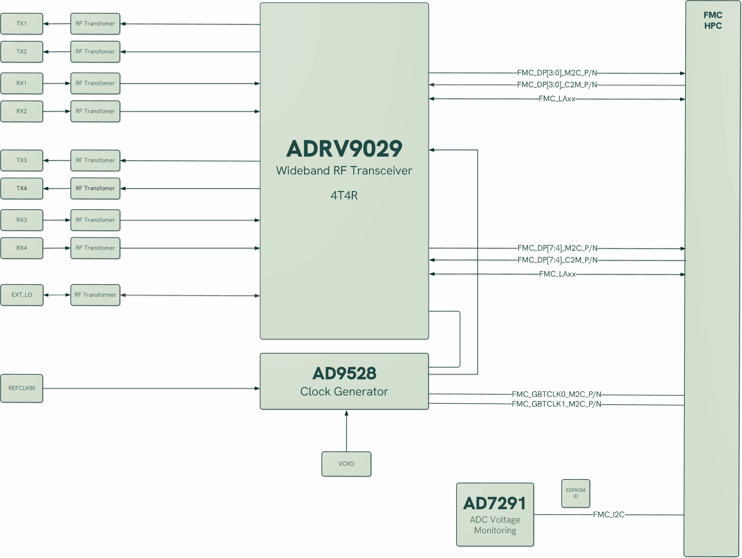
- RF Transceiver Analog Devices ADRV9029 based FMC
- Vita 57.1-2010 specification compliant
- FMC High Pin Connector (HPC)
- JESD024B/C interface up to 24.33 Gbps
- 4x Tx Lanes
- 4x Rx Lanes
- LA Bus LVDS and Singled-Ended
- Operates with VAdj = 2.5V to 1.5V
- Air and Conduction Cooled compatible
- Quad Transmitters (Tx)
- Quad Receivers (Rx)
- Ext_Lo Input/Ouput
- External Reference Clock Input
- RF Coverage: 75MHz to 6.0 GHz
- Tx Synthesis Bandwidth Max: 450MHz
- Rx Bandwidth Max: 200MHz
- Support Time Division Duplex (TDD)
- Support Frequency Time Division (FTD)
- Fully integrated independent fractional-N radio frequency synthesizers
- On-board VCXO : 100.000MHz, 122.880MHz, 125.000MHz, 153.600MHz or 156.250MHz
- Air Cooled and Conduction Cooled
Typical Applications
- Software Defined Radio
- Electronic Warfare
- Wireless Infrastructure 3G/4G/5G
- TDD and FDD active Antenna Systems
- Drones and UAVs
- Military Communications
Description
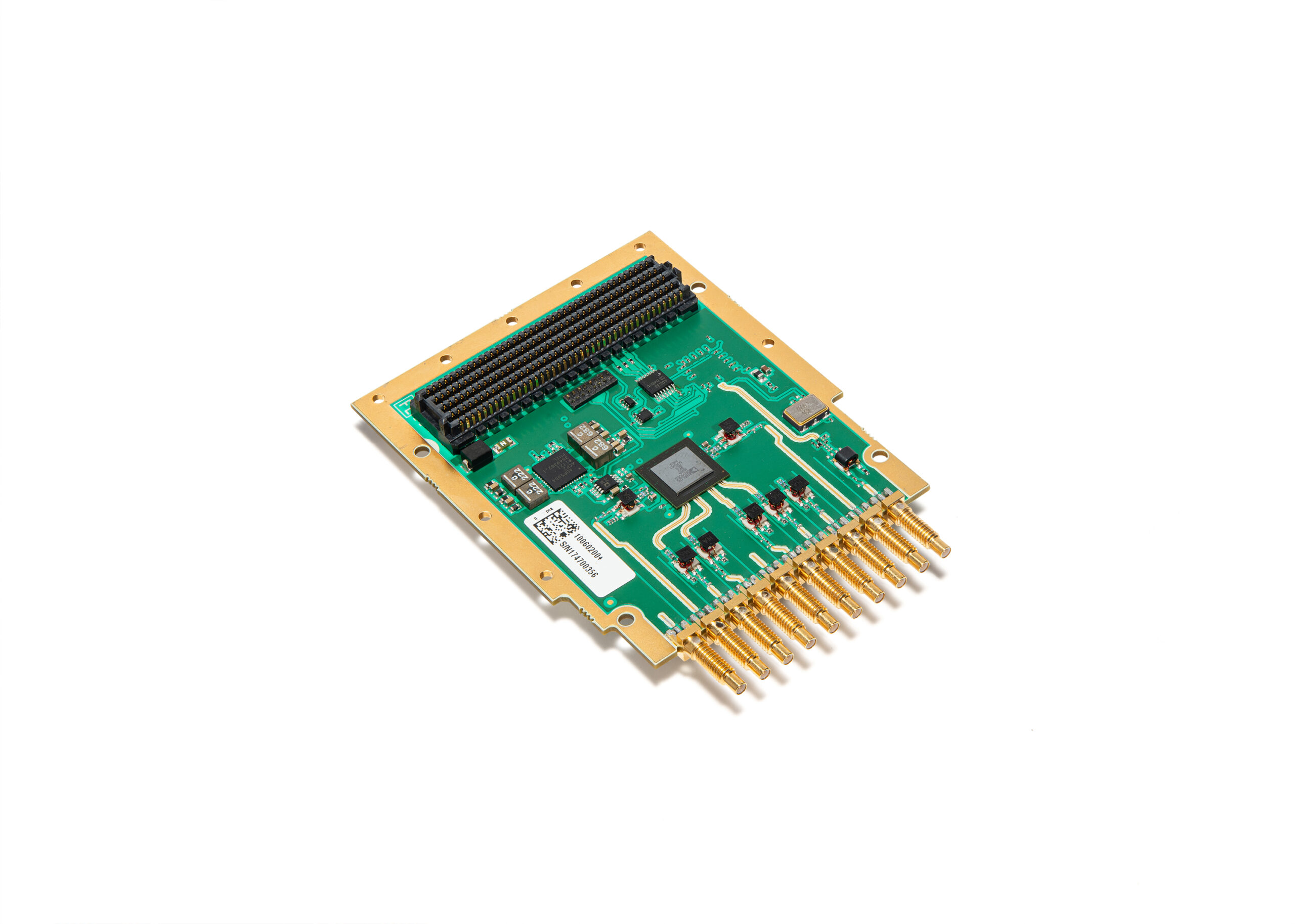
The FMC-ZU3RF-A is a FMC for RF wireless communications applications based on the ADRV9029 component from Analog Device Inc (ADI).
The ADRV9029 is a highly integrated, radio frequency (RF) agile transceiver offering four independently controlled transmitters, dedicated observation receiver inputs for monitoring each transmitter channel, four independently controlled receivers, integrated synthesizers, and digital signal processing functions providing a complete transceiver solution.
The device provides the performance demanded by cellular infrastructure applications, such as small cell base station radios, macro 3G/4G/5G systems, and massive multiple in/multiple out (MIMO) base stations.
The receiver subsystem consists of four independent, wide bandwidth, direct conversion receivers with wide dynamic range.
The four independent transmitters use a direct conversion modulator resulting in low noise operation with low power consumption. The device also includes two wide bandwidth, time shared, observation path receivers with two inputs each for monitoring transmitter outputs. The complete transceiver subsystem includes automatic and manual attenuation control, dc offset correction, quadrature error correction (QEC), and digital filtering, eliminating the need for these functions in the digital baseband.
Other auxiliary functions such as analog-to-digital converters (ADCs), digital- to-analog converters (DACs), and general-purpose input/ outputs (GPIOs) that provide an array of digital control options are also integrated. To achieve a high level of RF performance, the transceiver includes five fully integrated phase-locked loops (PLLs). Two PLLs provide low noise and low power fractional-N RF synthesis for the transmitter and receiver signal paths.
A third fully integrated PLL supports an independent local oscillator (LO) mode for the observation receiver. The fourth PLL generates the clocks needed for the converters and digital circuits, and a fifth PLL provides the clock for the serial data interface. A multichip synchronization mechanism synchronizes the phase of all LOs and baseband clocks between multiple ADRV9029 chips.
All voltage controlled oscillators (VCOs) and loop filter components are integrated and adjustable through the digital control interface. This device contains a fully integrated, low power digital predistortion (DPD) adaptation engine for use in power amplifier linearization. DPD enables use of high efficiency power amplifiers, reducing the power consumption of base station radios while also reducing the number of SERDES lanes necessary to interface with baseband processors.
PanaTeQ offers the VPX3-ZU1B-SDR-D development system based on the VPX3-ZU1B 3U OpenVPX Zynq Ultrascale+ and the FMC-ZU3RF-A-W1A-AS for typical Software Defined Radio application, in both air-cooled and conduction cooled version.
