FMC Mezzanine
Wideband RF Transceiver
Analog Devices AD9375

specifications
- Vita 57.1-2010 specification compliant
- FMC High Pin Connector (HPC)
- JESD024B interface up to 6144 Mbps
- LA Bus LVDS and Singled-Ended
- Operates with VAdj = 2.5V to 1.5V
- Air and Conduction Cooled compatible
- Fully ADRV9375 HW/SW compatible
- Dual Transmitters (Tx)
- Dual Receivers (Rx)
- Observation Receiver (ORx) with 2 inputs
- Fully integrated ultralow power DPD actuator and adaptation engine for PA linearization
- Sniffer Receiver (SnRx) with 1 input
- TX Ext LO Input/Output
- RX Ext LO Input/Output
- Reference Clock Input or Output
- FPGA GPIO direct Input or Output
- RF Coverage 300 MHz to 6.0 GHz
- Tx Synthesis Bandwidth (BW) to 250 MHz
- Rx Bandwidth: 7 MHz to 100 MHz
- Support Time Division Duplex (TDD)
- Support Frequency Division Duplex (FDD)
- Fully integrated independent fractional-N radio frequency synthesizers
- On-board VCXO : 100.000 MHz, 122.880 MHz, 153.600 MHz or 156.250 MHz
Typical Applications
- Software Defined Radio
- Wireless Infrastructure 3G/4G
- FDD and TDD active Antenna Systems
- Electronic Warfare
- Drones and UAVs
Description
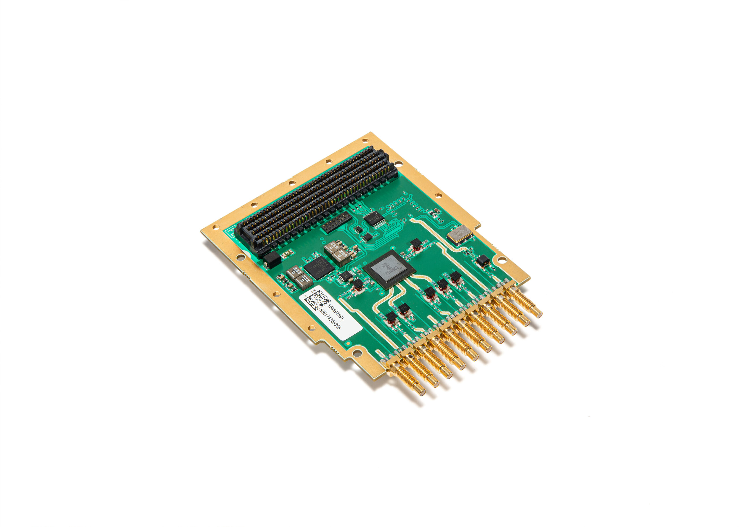
The FMC-ZU1RF-B is a FMC for RF wireless communications applications based on the AD9375 component from Analog Device Inc (ADI).
This FMC is fully hardware and software compatible with the ADRV9375 evaluation board from ADI.
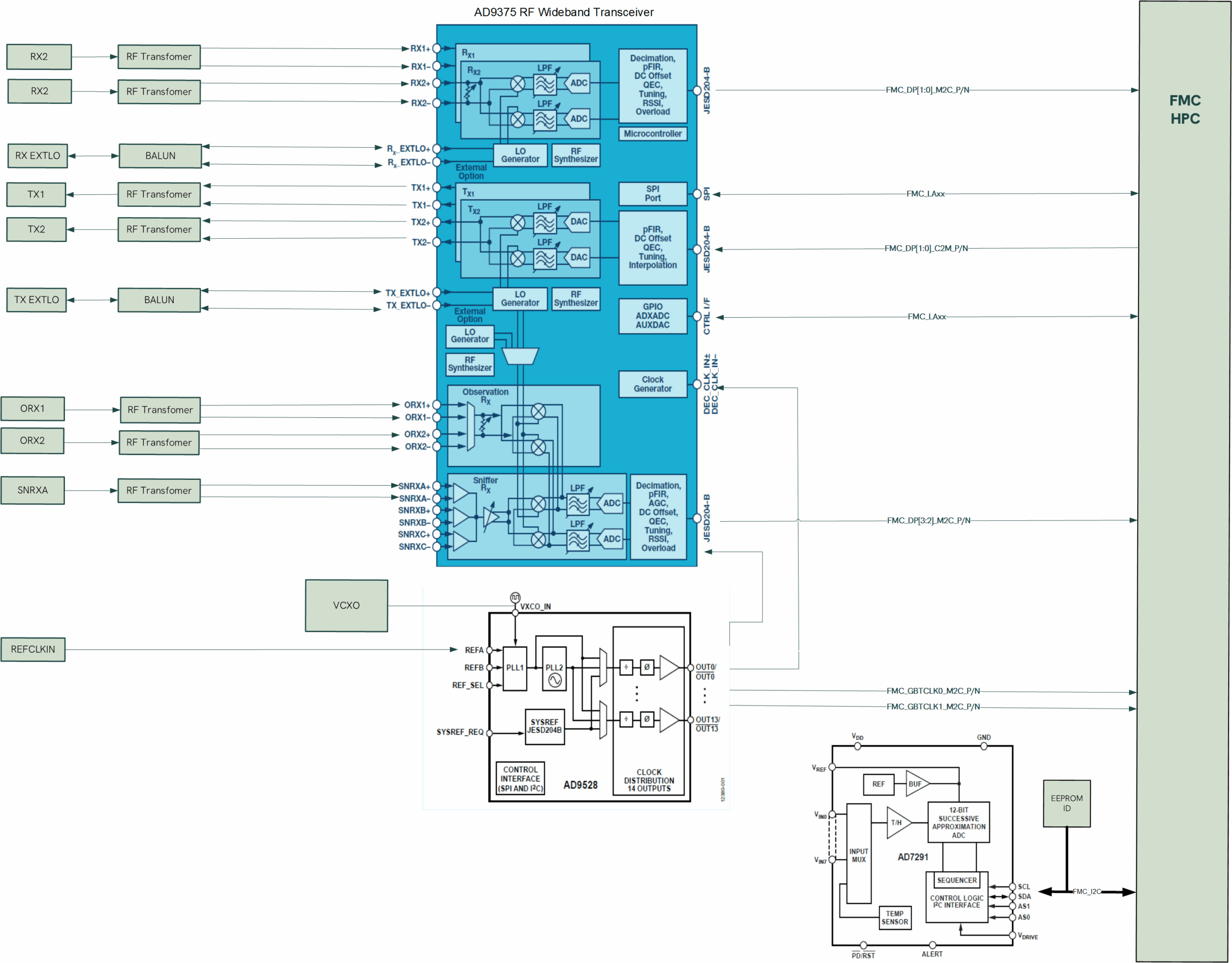
The AD9375 component is a highly integrated, wideband RF transceiver offering dual channel transmitters and receivers, integrated synthesizers, a fully integrated digital predistorsion (DPD) actuator and adaptation engine, and digital signal processing functions. The IC delivers a versatile combination of high performance and low power consumption required by 3G/4G micro and macro base station equipment in both FDD and TDD applications.
The AD9375 operates from 300 MHz to 6000 MHz, covering most of the licensed and unli-censed cellular bands. The DPD algorithm supports linearization on signal bandwidth up to 40 MHz depending on the power amplifier (PA) charecteristics.
The IC supports receiver bandwidths up to 100 MHz. It also supports observation receiver and transmit synthesis bandwidths up to 250 MHz to accommodate digital correction algorithms.
The transceiver consists of wideband direct conversion signal paths with state-of-the-art noise figure and linearity. Each complete receiver and transmitter subsystem includes dc offset correc-tion, quadrature error correction, and programmable digital filters, eliminating the need for these functions in the digital baseband.
Several auxiliary functions such as an auxiliary analog-to-digital converter (ADC), auxiliary digital-to-analog converters (DACs), and general-purpose input/outputs (GPIOs) are integrated to provide additional monitoring and control capability.
An observation receiver channel with two inputs is included to monitor each transmitter output and implement interference mitigation and calibration applications. This channel also connects to three sniffer receiver inputs that can monitor radio activity in different bands.
The high speed JESD204B interface supports lane rates up to 6144 Mbps. Four lanes are dedicated to the transmitters and four lanes are dedicated to the receiver and observation receiver channels.
The fully integrated phase-locked loops (PLLs) provide high performance, low power fractional-N frequency synthesis for the transmitter, the receiver, the observation receiver, and the clock sections. Careful design and layout techniques provide the isolation demanded in high perfor-mance base station applications. All voltage controlled oscillator (VCO) and loop filter components are integrated to minimize the external component count.
